Anchor
From Hackstrich
Anchor will be an electronic current/voltage sink, for testing/characterizing power supplies and other similar tasks.
Status
- 2012-01-29: Too many projects on the go, this one's getting put into dormant state for now.
- 2011-10-30: Realized that the output FET's Vgs(th) is outside the range the op-amp can put out. Need to redesign the output section.
- 2011-10-29: Output DAC working, but op-amp buffer is outputting 2.5V no matter what the input is. Other op-amp channel (current sense) seems to work okay though, so unsure what is causing this.
- 2011-10-28: Code cleanup and modularizing (still just local, not committed yet).
- 2011-10-27: vADC SPI fully working, buzzer working.
- 2011-10-26: Parts arrived and installed. TFT still not working, but RS232 transmission works. Work on vADC SPI is in progress.
- 2011-10-25: More work on the TFT, no progress. Eric has ordered the ADC, DAC, and TFT connector I need.
- 2011-10-23: More work on the TFT, 6 hours with the scope yielded no further progress.
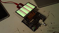
- 2011-10-22: Got border test working (PIC generates coloured lines around the perimeter of the TFT) but colour bar test is not working, coming up with ~30 yellowish-red bars instead of the expected 8 colours.
- 2011-10-21: Brought up board and programmed it for the first time, found issue with TFT FPC connector (worked around) and backlight driver (worked around). Now board programs, controls load relay, and lights up TFT backlight. Asked Eric to add a A100226CT-ND to his next order, BOM is not updated yet until I verify the new part fits/works.
- 2011-10-20: Mostly assembled first Anchor logic board, except for DAC (wrong pkg), vADC (missed ordering), and heat sink (will add later once low-power tests are done). TFT is arriving tomorrow evening. Have put a request in with Eric to order the missing parts in his next order (mid-next week).
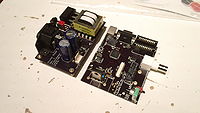
- 2011-10-18: Received Anchor logic board PCBs.
- 2011-10-15: Fixed most of the known issues with the rev. 1 PSU board.
- 2011-10-13: Built first Anchor PSU board, works as designed, putting out 3.3v! There are a couple very minor issues which have been noted here.
- 2011-10-12: Parts for Anchor PSU and logic board have been received.
- 2011-10-09: Anchor PSU PCB received, order placed for all PSU and logic board parts.
- 2011-09-22: Tagged as rev. 1 and sent to Laen for PCB manufacturing. Parts still need to be ordered.
- 2011-09-21: Added speaker and completed the rest of the routing. Added silkscreen to all connectors/test points/button/etc. One final check tomorrow, then will be sent to Laen.
- 2011-09-19: Completed rev. 1 schematic, started working on board layout and got about 80% completed, remaining to complete are the USB port, one of the two expansion slots, and GND.
- 2011-09-18: Worked on schematic, completed the two ADC sections and the DAC section for measurement and load driving.
- Pre-September 2011: Put together majority of desired specs and started putting BOM together, put together UI part of the schematic.
Specs/Brainstorming
- Desired features/specs:
- Constant current and constant voltage options
- Maybe constant power too?
- Ramp-up/down automatically and track outputs
- Pulse load to test transient response
- 5A/100V maximums
- 500W dissipation in a FET is a bit nuts, so it won't be 5A *at* 100V
- 100W continuous, 500W pulse might be reasonable? Would be nice anyway.
- Some kind of computer interface for more complicated tests/more detailed data analysis
- USB would be easy to implement
- Implemented on rev. 1
- RS232 would be even easier to implement
- Implemented on rev. 1
- Ethernet could be cool, but that seems overkill here
- The LXI standard seems useful for this, could be implemented on an expansion card
- GPIB would be the traditional choice for test gear, but I've never done any work with it
- Could be implemented on an expansion card later if there is any need
- USB would be easy to implement
- Add-on module system for adding extra monitoring channels for things that might be expensive to implement or not commonly used
- Temperature monitoring (a couple channels worth) would be good, as you often want to monitor chips/pass elements/etc. while load testing supplies
- Everything to do with thermocouples is expensive, so making this an add-on module would be good
- Temperature monitoring (a couple channels worth) would be good, as you often want to monitor chips/pass elements/etc. while load testing supplies
- Direct connection to mains, as power bricks are annoying in hackerspaces where gear is moved around a lot
- Constant current and constant voltage options
- PIC24FJ256DA210 will be used as it has all the graphics/LCD drive/acceleration built in to enable a nice colour TFT display
- Inputs
- Digital
- Load On/Off
- Event trigger switch
- CC/CV mode?
- 3 for UI quadrature encoder
- 2 for touchscreen
- MCU-integrated 10-bit ADC
- Heatsink temperature
- 2 for touchscreen
- Digital
- Outputs
- Digital
- CC/CV mode relay (if required)
- Scope trigger output
- Load disconnect relay
- 3x SPI /SS outputs
- Digital
- Communication Busses
- I2C
- AR1020 I2C resistive touchscreen controller (will try to eliminate it and do it in the PIC for revision 2)
- SPI
- 2x LTC2450 SPI 16-bit ADC for current and voltage measurement
- 1x MCP4921 12-bit DAC for driving the MOSFET
- I2C
- Inputs
- Want a graphical LCD for the output/UI, and the PIC chosen will drive a nice TFT
- WQVGA is a nice size, can get a menu/buttons on the side and still have room for the info display
- The Newhaven NHD-43-480272MF-ATXI-T-1 from Mouser seems the best option for size/touch/resolution
Revision 1 Issues
PSU
- Fixed on rev. 2 -
Fuse holder pins are bigger than holes - IEC connector ground tab would interfere with caps if anything was connected to it
- Fixed on rev. 2 -
Up on power switch is off, down is on - Fixed on rev. 2 -
Plastic on output connector covers URL - Added on rev. 2 -
No power LED on the board
Logic Board
- Silkscreen for U7 and U8 is on wrong layer so not on PCBs
- Silkscreen missing on SW1
- No test points for backlight voltage
- Fixed on BOM -
R10, R11 missing from BOM - Fixed on BOM -
One ADC missing from BOM qty-wise - Fixed on BOM to SOIC8 version -
U8 (output DAC) footprint is SOIC8, chip is MSOP - No LEDs for power or status included
- K1 silkscreen doesn't match part, so relay overlaps Q2
- SW1 is facing inwards instead of out the front panel!
- SW1 is missing silkscreen
- SW2 is comedically tiny
- Second copy of 'rev. 1' text under LCD connector
- C21 footprint is bigger than actual part
- TFT FPC connector is top-contact type, needs to be bottom-contact type
- CTRL pin on U6 is floating, which shuts down backlight driver
- Slot 1 is labeled 'Slot 2' and vice-versa

